Data Retention Voltage and LDO Design: Ensuring Reliability Under Unstable Residual Voltage Conditions
This article explains the challenges of data retention voltage and LDO design for SRAM. It outlines error factors in low-voltage environments and measures to protect equipment reliability. Furthermore, it introduces the option of utilizing non-volatile memory as a solution.
Relationship between SRAM Data Retention Voltage (VDR) and LDO Design
The data retention voltage for SRAM is a crucial design metric indicating the minimum voltage requirement necessary for volatile memory to safely retain data while powered. The LDO plays a vital role in stably supplying this voltage, and particularly in preventing it from falling below the retention voltage during power supply fluctuations. The two factors are closely linked and significantly impact the overall reliability of the power supply design.
What is Data Retention Voltage and its Design Importance?
Data retention voltage (VDR) refers to the minimum power supply voltage at which a memory cell can maintain written information without loss. This value is affected by process variations, temperature conditions, and leakage current, so sufficient margins must be ensured during design. Especially in SRAM, a drop below the retention voltage immediately results in data corruption, directly impacting system reliability. Therefore, in power supply designs with backup modes, protective design measures based on this voltage are essential.
Concept of Voltage Margin in SRAM
In SRAM design, it is essential to ensure a voltage margin that accounts for not only the ideal retention voltage but also the worst-case scenario. Actual operating voltages fluctuate due to process variations, temperature fluctuations, and power supply noise; therefore, statistical distributions must be considered rather than simple specification values. Furthermore, it is crucial to define the safe operating region in real-world environments by taking into account LDO output errors and instantaneous voltage dips caused by sudden load changes.
Mechanism of Data Retention Errors Occurring During Power Supply Drops
When the power supply voltage drops, the flip-flops within the memory cell become less able to hold their state, leading to unstable logic state identification. In this state, the device becomes more susceptible to noise and leakage current, resulting in bit inversion and data loss. Especially when the power supply drops gradually, the LDO enters the dropout region, and the output becomes unable to keep up, resulting in longer periods below the retention voltage. Such transient voltage instability regions are the main cause of data corruption in actual field applications.
Challenges of Low-Voltage and Residual-Voltage Operation in LDO Design
While LDOs can maintain a stable output when the input voltage is sufficient, their performance is significantly limited in residual-voltage environments. In particular, as the input voltage drops and the device enters the dropout region, output controllability decreases, making it difficult to maintain the hold voltage. Understanding the behavior under these conditions is key to reliable design.
Dropout Voltage and Headroom Constraints
In an LDO, the dropout voltage is a crucial parameter that defines the minimum difference between the input and output voltages. This constraint directly impacts performance in residual voltage environments. When the input voltage drops and headroom becomes insufficient, the pass element turns completely on, causing the control loop to lose regulation. As a result, the output voltage simply follows the input voltage, making stable voltage supply impossible. Furthermore, rising ambient temperature can worsen dropout characteristics, making it essential to design with a margin that anticipates worst-case conditions.
Output Instability Factors During Input Voltage Drop
As the input voltage drops, the LDO’s internal control loop gradually approaches its operating limit, compromising output voltage stability. In particular, a decrease in loop gain and phase margin makes output ripple and oscillation more likely. Additionally, when load fluctuations occur, output voltage dips are amplified, increasing the risk of momentarily falling below the retention voltage. Furthermore, if the input power supply itself has noise or fluctuations, these are more easily propagated to the output, affecting the overall system reliability.
Low-Voltage Operating Limits of Error Amplifiers and References
The error amplifiers and bandgap references that support the accuracy of LDOs are designed to operate above a certain voltage. Therefore, when the input voltage drops, these circuits may not function properly, and the accuracy of output voltage control deteriorates rapidly. In particular, if the reference voltage becomes unstable, the output voltage itself may deviate from the design value, increasing the risk of it falling below the retention voltage. Also, at low voltages, the effects of offset and noise become relatively larger, so it is important to understand the operating limits at the design stage and ensure an appropriate safety margin.
Data Retention and Reliability Assurance Techniques under Unstable Residual Voltage Conditions
In environments with unstable residual voltage, countermeasures are required not only for the performance of the LDO itself, but also for the entire power supply system. In particular, designing the system to prevent the voltage from falling below the holding voltage during transient fluctuations such as power dips and momentary interruptions is crucial. By combining multiple design techniques, it is possible to ensure data retention reliability in real-world environments.
Ensuring Reliable Operation During Power Dips and Momentary Interruptions
To maintain data retention even when power dips or momentary interruptions occur, designing to control the rate of voltage drop (discharge) is essential. Specifically, placing capacitors with sufficient capacity on both the input and output sides increases the time constant, extending the time before the voltage falls below the retention voltage. Furthermore, considering the transient response characteristics of the LDO, it is necessary to configure the system to maintain a stable output even under steep load fluctuations. Additionally, designing the system to sleep the microcontroller before entering a dangerous voltage range, in conjunction with a power supply monitoring circuit, is also effective.
Voltage Stabilization Utilizing PSRR and Transient Response
PSRR is an important indicator showing how much input power supply noise and ripple affect the output, and its importance increases even further in residual voltage environments. By selecting an LDO with high PSRR characteristics, fluctuations in input voltage can be suppressed, ensuring output voltage stability. Furthermore, LDOs with excellent transient response performance can suppress voltage dips even in the face of rapid load changes, making them effective in maintaining the retention voltage. It is crucial to comprehensively evaluate these characteristics and select a device suitable for the application.
Decoupling and Power Sequence Design
Appropriate placement of decoupling capacitors is essential for reducing power line impedance and absorbing instantaneous voltage fluctuations. Placing them particularly close to the memory’s power pins can improve local voltage stability. Power sequence design allows for control of voltage supply timing to each block, preventing malfunctions in unstable conditions. Combining these techniques maintains a high level of system reliability even in residual voltage environments.
The Potential of Non-Volatile Memory and the Option of FRAM
To fundamentally improve data retention reliability, an approach that reconsiders the selection of the memory device itself, in addition to voltage maintenance by LDOs, is also effective. Especially with the increasing miniaturization and resulting lower voltage requirements, the conventional SRAM + backup power configuration is approaching its design limits.
Limitations of Data Retention Design Using SRAM + LDO
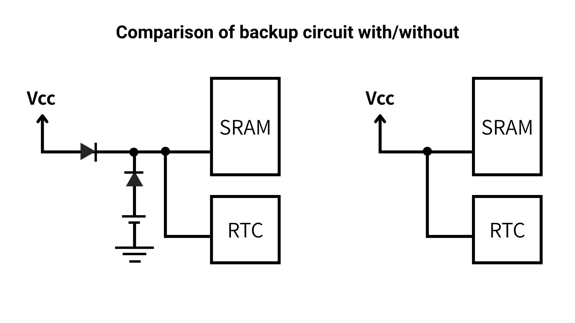
In data retention designs using SRAM, managing the lifespan of backup batteries, the mounting area of large-capacity capacitors, and the extremely precise voltage control of LDOs are always challenges. In particular, designs that maintain a standby current of several microamperes for years lead to increased component count and higher costs. Furthermore, it is difficult to completely eliminate the risk of data loss due to even slight noise in the power supply voltage, leading to a growing demand for simpler and more robust data retention methods.
Characteristics of Non-Volatile Memory that Eliminates the Need for Retention Voltage (VDR)
Non-volatile memory can retain data even when the power supply is completely cut off (becomes 0V), eliminating the need for VDR management, which was a challenge with SRAM. This allows for significant simplification or elimination of advanced residual voltage control and backup circuits using LDOs. Rather than relying on the traditional design philosophy of protecting data at the moment of power loss, leveraging the physical property of retaining data with no power at all makes it possible to achieve both reduced system power consumption and improved reliability.
The Potential of FRAM with Rewrite Endurance Equivalent to SRAM
The biggest hurdle in the transition to non-volatile memory is “rewrite endurance,” but FRAM (FeRAM, ferroelectric memory) solves this problem. Unlike Flash and EEPROM, FRAM offers high-speed writing equivalent to SRAM and virtually unlimited rewrite endurance exceeding 10 trillion cycles. Unlike SRAM, FRAM does not require a retention power supply, and it can withstand high-frequency logging, making it an extremely powerful option for data protection in unstable power environments.
RAMXEED Parallel Interface FeRAM Family
RAMXEED Quad SPI Compatible FeRAM Family