This article covers high-speed data transfer techniques using QSPI (Quad SPI), including protocol architecture, XIP utilization, DMA integration, and circuit design. It details practical approaches to improving performance in embedded development.
QSPI Fundamentals and the Theory Behind High-Speed Operation
QSPI is a serial communication interface that extends SPI by enabling high-speed data transfer using up to four data lines. It is commonly used for communication between external flash memory and microcontrollers(MCUs), contributing significantly to reduced boot times and improved responsiveness in real-time applications. As modern embedded systems increasingly demand faster code execution and data access, QSPI has become a widely used solution for meeting these performance requirements.
What Is QSPI? Fundamental Differences from SPI
QSPI is an enhanced version of conventional SPI that can achieve up to four times the theoretical transfer rate by using as many as four data lines. QSPI communication consists of three phases: command, address, and data. The number of data lines used in each phase can be configured independently, offering flexibility in communication design. This architecture allows developers to select the most suitable communication mode based on the capabilities of the flash memory and microcontroller in used, thereby improving transfer efficiency. In embedded systems, QSPI is widely utilized for applications such as direct code execution and high-speed access to large volumes of data.
QSPI I/O Architecture and High-Speed Transfer MechanismsQSPI
achieves higher throughput than conventional SPI by increasing the number of bits transferred per clock cycle through the use of multiple data lines. While standard SPI transfers one bit per clock cycle using a single data line, QSPI can transfer up to four bits per clock cycle using four data lines simultaneously. Another characteristic of QSPI is the ability to independently configure the transfer method and bit width for the command, address, and data phases. This flexibility enables designers to optimize transfer configurations according to system characteristics and application requirements, achieving both higher performance and improved efficiency.
Protocol Variants (Quad / QIO / QPI)
QSPI supports three primary communication modes: Quad, QIO (Quad I/O), and QPI (Quad Peripheral Interface). In Quad mode, commands and addresses are transmitted over a single data line, while data is transferred using four data lines. In QIO mode, the address phase also uses four-line transmission. In QPI mode, all phases—including command, address, and data—are transferred using four data lines. QPI offers the highest performance but requires support from both the microcontroller and flash memory device. Understanding the characteristics and compatibility requirements of each mode is essential for selecting the most appropriate communication method based on system requirements, communication speed targets, and implementation constraints.
Implementation Techniques for Higher Performance
Maximizing QSPI performance requires more than simply enabling quad transfers. It involves combining multiple optimization techniques, including transfer timing adjustments, memory-mapped access, and DMA integration. Since performance bottlenecks vary depending on flash memory characteristics and overall system architecture, optimization strategies should be tailored to specific implementation requirements.
Optimizing Dummy Cycles and Wait Cycles
When reading data from QSPI flash memory, dummy cycles are required to ensure stable data output. However, excessive dummy cycle settings introduce unnecessary latency and reduce performance. Conversely, too few dummy cycles can result in data corruption. Proper tuning based on the flash memory specifications is therefore essential. Configuring the appropriate number of dummy cycles according to clock frequency and I/O mode, followed by validation on actual hardware, is often the first step toward improving QSPI performance.
XIP (Execute In Place) for Faster Memory Access
XIP (Execute In Place) enables code stored in QSPI flash memory to be executed directly from external flash without first being copied into RAM. This approach reduces RAM usage while shortening system startup times. When a QSPI interface supports memory-mapped mode, the CPU can access external flash as if it were ordinary memory, allowing XIP to function effectively. However, implementation constraints such as cache coherency and interrupt handling alignment must be carefully managed, as they can affect both performance and system stability.
DMA Transfers and Cache Design Considerations
DMA is highly effective for continuous transfers of large amounts of data through QSPI. By using DMA, data can be transferred directly from flash memory to RAM without CPU intervention, allowing the CPU to perform other tasks concurrently. In addition, using cache management on the destination memory region can reduce access latency during data reuse and improve overall processing efficiency. Finding the right balance between DMA configuration and cache design is a critical factor in successful QSPI performance optimization.
Platform-Specific Performance Optimization
To fully utilize QSPI performance, it is necessary to understand platform-specific limitations and optimization points during design and implementation. In particular, since QSPI control methods and peripheral circuit constraints vary depending on the MCU or FPGA, the approach must match the device specifications..
Optimizing QSPI Clock Configuration in MCUs
In microcontroller-based systems, QSPI clock configuration has a significant impact on communication performance. The QSPI clock frequency must be selected based on both the flash memory specifications and the limitations of the peripheral interface. Exceeding the maximum operating frequency of the flash memory can cause data corruption, while operating below optimal frequencies limits performance. Maintaining clock integrity also requires careful configuration of PLL settings and bus clock dividers. Thorough validation during the design phase and robust timing design across the entire system are essential for achieving high-speed and reliable communication.
QSPI Controller IP and Circuit Design Considerations
When implementing QSPI in an FPGA or custom SoC, it is important to understand the functional limitations and timing specifications of the selected QSPI controller IP. Insufficient clock domain isolation or poor timing closure can lead to intermittent data corruption and XIP execution failures. At the PCB level, designers must also pay attention to physical-layer considerations such as impedance matching, trace length matching, and termination strategies. As transfer speeds increase, signal integrity issues including edge-rate effects and reflections become increasingly significant, making validation from both hardware and logic design perspectives essential.
Real-World Examples of Accelerated Display Processing and Data Transfer
As a concrete example demonstrating the practical performance benefits of QSPI, we present a successful case involving display processing and data transfer. In a system that achieved 60 FPS LCD rendering using QSPI, the key success factors were DMA transfers, cache management, and timing optimization. Image data was stored in QSPI flash memory and transferred to RAM via DMA, while cache utilization reduced bus traffic. In addition, synchronization between frame refresh timing and DMA triggering enabled high-speed rendering without display flicker. This example illustrates that realizing the full performance potential of QSPI requires coordinated optimization of both hardware and software.
Key Design Considerations for Leveraging QSPI Performance
Effective QSPI optimization requires a comprehensive approach that spans physical-layer design, firmware architecture, and system-level configuration. Designers should iteratively validate and optimize I/O architecture, transfer methods, cache management, and clock design based on actual hardware validation and the specific constraints of their applications.
Summary of Key QSPI Optimization Techniques
Achieving high-performance QSPI communication begins with selecting the appropriate I/O configuration between the flash memory and microcontroller. Additional optimization techniques include tuning dummy cycles, enabling XIP, integrating DMA transfers, and optimizing cache behavior. Clock configuration and register settings should also be tailored to the capabilities of the target platform. Since performance improvements rarely result from a single technique, successful optimization requires integrating multiple approaches while balancing subsystem-level and system-level considerations.
Common Causes of Performance Degradation and Countermeasures
When QSPI performance falls short of expectations, common causes include incorrect dummy cycle settings and improper cache configuration. Throughput can also be reduced by DMA configuration issues, bus contention, and interrupt processing overhead. Signal integrity problems such as reflections and crosstalk caused by external flash connections can further impact performance. Addressing these issues typically requires iterative design and validation, including timing analysis with signal and timing analysis tools, cache configuration reviews, and adjustments to bus arbitration settings.
Future Trends and Application Opportunities for QSPI
QSPI is expected to remain an important interface for high-speed access to external memory. It is becoming increasingly important in applications such as edge AI processing, OTA (Over-the-Air) updates, and graphics-intensive systems, where rapid data access is essential. Future developments are likely to include broader adoption of Octal SPI interfaces and expanded use of QSPI in secure boot implementations. Continued refinement of existing techniques, together with the development of design methodologies for emerging applications, will further enhance the value and versatility of QSPI technology.
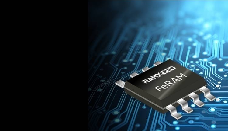
RAMXEED Quad SPI Supporting FeRAM Product Lineup