How Non-Volatile Memory Works: Mechanisms by Memory Type
Author Information
Takashi Eshita, Ph. D.
Senior Expert, RAMXEED Co., Ltd.
Non-volatile memory is a type of memory that retains data even when the electric power is turned off. There are various types of non-volatile memory, and the mechanism for data-storage without power differs depending on the memory type. This article explains the data-storage mechanisms and read/write operations of different types of non-volatile memory other than FeRAM (Ferroelectric Random Access Memory).
For the operating principles of FeRAM, please refer to the following page.
FeRAM Features, Principles, and Basic Operation
ReRAM
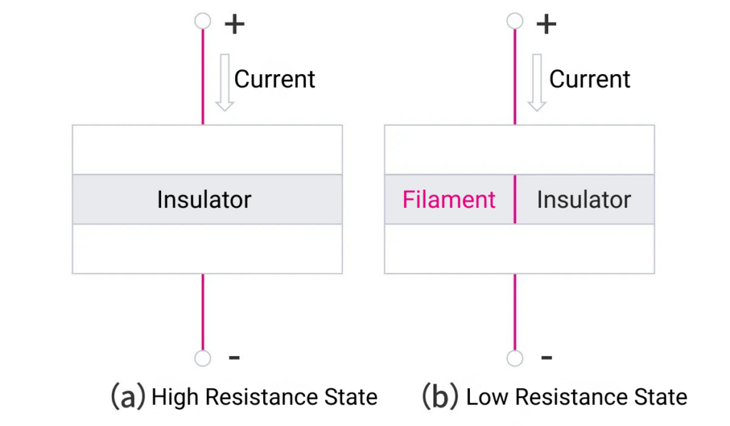
ReRAM (Resistive Random Access Memory) stores information by utilizing resistive switching in an insulating material, such as a metal oxide (e. g. tantalum oxide or hafnium oxides) placed between two electrodes (Figure 1) [2].
When voltage is applied between the two electrodes, the insulating material in the high-resistance (HR) state transitions to a low-resistance (LR) state by forming a conductive path, called a “filament” at a certain voltage.
When the voltage is increased further, the filament disappears, and the insulating material in the LR state returns to its original HR state. In unipolar type ReRAM, this process is caused by excessive current, which generates heat and eventually melting the conductive filament. In bipolar type ReRAM, which is a current mainstream approach, reversing the electrode polarity returns the LR state to the original HR state where oxidation-reduction reactions are the primary mechanism for the disappearing of the conducting filament rather than filament melting.
To read information, a voltage lower than the write voltage is applied across both electrodes, and the resulting current is measured.
Because rewriting the stored data requires applying a high voltage and allowing a large current to flow, ReRAM functions as non-volatile memory.
In addition to this operating mechanism, some ReRAM devices operate by generating HR and LR states through changes in Schottky barrier height or oxidation-reduction reactions at the interface between the electrode and the insulating material.
PCRAM
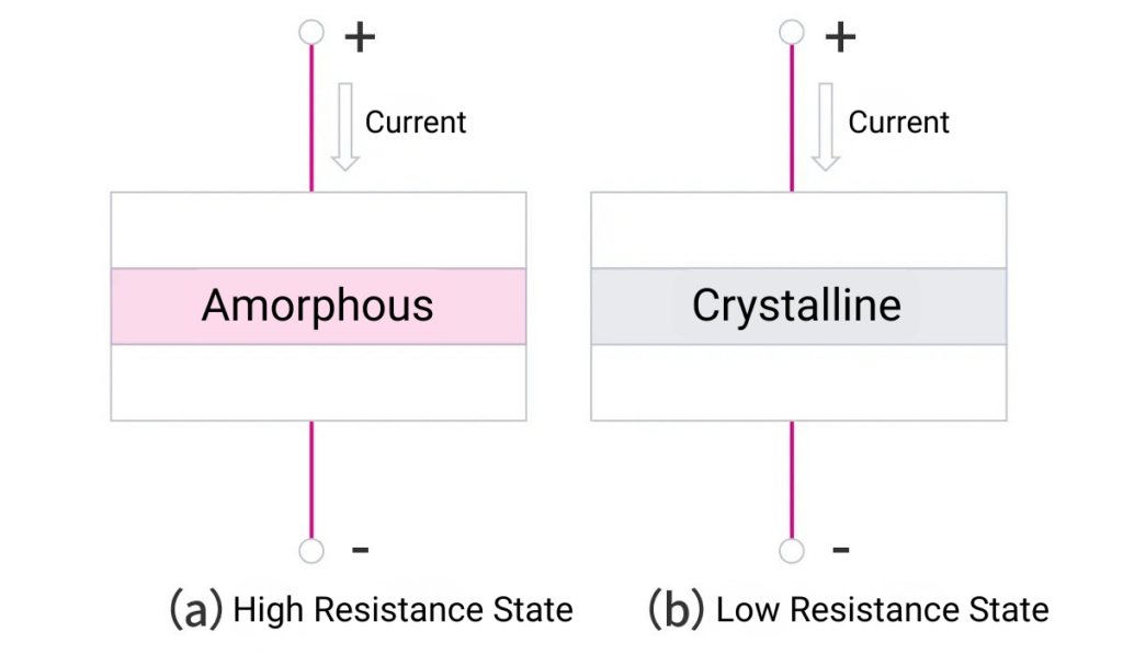
PCRAM (Phase Change Random Access Memory) stores information by utilizing changes in the resistance of insulating materials such as chalcogenides, typically Ge2Sb2Te5, placed between two electrodes (Figure 2) [3].
Such insulating materials exhibit the amorphous state corresponding to an HR state, in which the constituent elements are arranged randomly like glass, and crystalline state corresponding to a LR state.
To write information, the current through the chalcogenide is controlled by applying voltage across the electrodes to regulate the heating and cooling rate, slow heating results in the chalcogenide being in a crystalline state, whereas rapid heating followed rapid cooling produces an amorphous state.
To read information, a voltage lower than the write voltage is applied across both electrodes, and the resulting current is measured. As long as a current sufficient to raise the temperature is not applied, the stored data remains non-volatile.
In addition to chalcogenides, PCRAM sometimes uses superlattice structures composed of multiple alternating thin layers of GeTe and Sb2Te3.
Because PCRAM relies on thermal phenomena, it faces challenges such as high power consumption and errors caused by thermal interference between adjacent memory cells when densely integrated.
MRAM
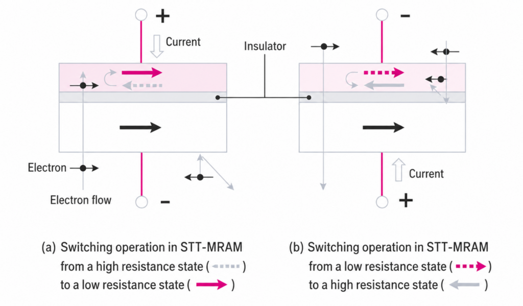
MRAM (Magnetoresistive Random Access Memory) is a type of non-volatile memory that utilizes this property (Figure 3) [4].
In a structure where a thin insulating layer (commonly MgO) is sandwiched between two magnets, the current flowing between the two magnets through the insulating layer (tunnel current) changes depending on the relative magnetization directions of the magnets. This phenomenon is known as the tunnel magnetoresistance effect.
When the magnetizations of the two magnetic layers are aligned in the same direction (parallel state), a large current can flow, resulting in a LR state. When the magnetizations are opposite (antiparallel state), only a small current flows, resulting in a HR state. Data writing is performed by changing the magnetization direction of one of the magnets.
There are mainly two methods for this. One is the toggle method, which uses the magnetic field generated by current flowing through adjacent wiring (toggle MRAM or simply MRAM). The other is the spin-transfer torque method (STT-MRAM), which uses the current flowing between the two magnetic layers.
The latter utilizes the property that electrons pass more easily when the direction of their magnetic spin matches the magnetization direction of the magnet they pass through.
When electrons are injected from below (left figure), only electrons whose spins align with the magnetization direction pass through the insulating layer and reverse the magnetization direction of the opposite magnet to match the spin direction. This is called spin-transfer torque.
Conversely, when electrons are injected from above (right figure), the spins of electrons that cannot pass through the lower magnet reverse the magnetization direction of the upper magnet, thereby rewriting the stored information.
To read information, a voltage lower than the write voltage is applied across both electrodes, and the resulting current is measured. As long as operations that rewrite the stored information are not performed, the data remains non-volatile.
In general, MRAM faces several challenges. External magnetic fields may rewrite stored information, toggle-type MRAM requires large currents to reverse magnetization, resulting in high power consumption, and in STT-MRAM, thermal effects may probabilistically prevent electron spins from reversing magnetization during writing, requiring additional techniques to ensure reliable rewriting.
Flash Memory and EEPROM
Flash memory and EEPROM are memory technologies that provide non-volatile data storage by accumulating charge in the gate region of a metal-oxide-semiconductor field-effect transistor (MOSFET).
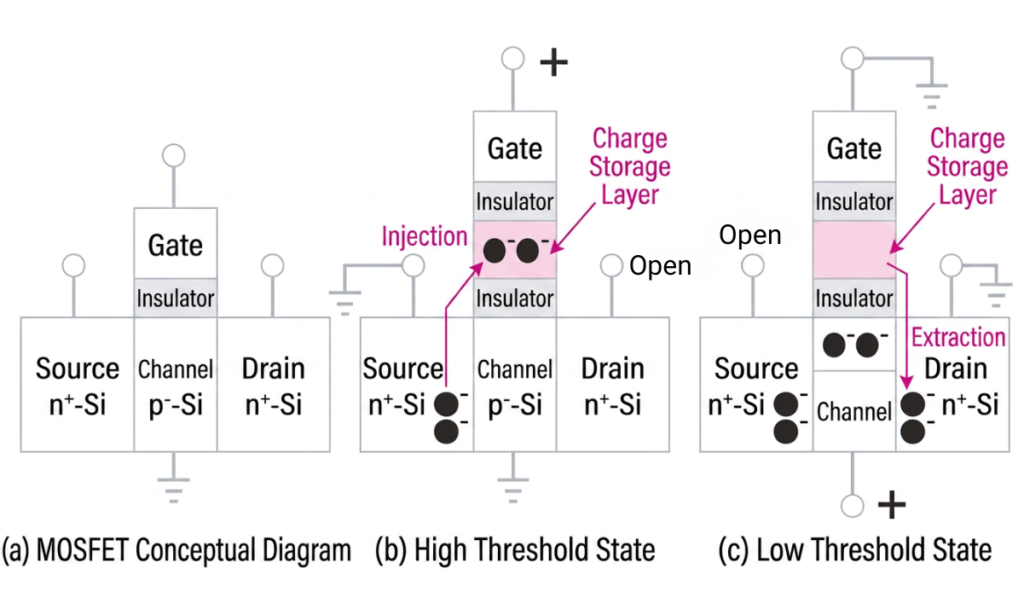
In a MOSFET, which is the dominant semiconductor transistor today (Figure 7(a)), voltage applied to the gate controls the resistance of the channel region and thereby controls the current flowing between the source and drain, enabling transistor operation.
Consider a MOSFET in which current begins flowing between the source and drain as positive voltage is applied to the gate. The gate voltage at which current starts flowing is called the threshold voltage.
Figures 4(b) and 4(c) show examples of memory cells for flash memory and EEPROM.
A charge storage layer is placed beneath the gate electrode (control gate) with an insulating film in between. When electrons are accumulated in the charge storage layer (Figure 4(b)), the threshold voltage of the MOSFET increases, and a higher gate voltage is required for current to flow between the source and drain.
When no electrons are stored in the charge storage layer (Figure 4(c)), the threshold voltage decreases, and current flows even at a lower gate voltage.
Flash memory and EEPROM store information using this difference in threshold voltage.
Data is rewritten by applying a high voltage between the control gate and the source or drain, causing electrons to be injected into or removed from the charge storage layer through the insulating film.
As long as high voltage is not applied to inject or remove electrons from the charge storage layer, the stored data remains non-volatile.
To read information, voltage is applied to the control gate, and the current flowing between the source and drain is measured to determine whether the threshold voltage is in a high or low state.
EEPROM uses such memory elements together with standard MOSFETs to form individual memory units.
Flash memory achieves high integration density by connecting only memory elements in series and writing or erasing data in groups.
Previously, memory devices that stored only two resistance states, high and low, were mainstream. Today, multiple bits can be stored in a single memory element by controlling the amount of charge accumulated in the charge storage layer across multiple levels.
Furthermore, memory cells that were previously arranged on a planar silicon wafer are now stacked three-dimensionally, enabling even larger storage capacities.
For planar memory cells, conductive materials using the floating-gate method were commonly used for the charge storage layer. In three-dimensional memory cells, insulating films are more commonly used [1,5].
Both flash memory and EEPROM face several challenges. Because electrons pass through the insulating film during rewriting, the dielectric endurance of the film gradually deteriorates, limiting rewrite endurance to approximately 105 programming/erasing cycles. In addition, high voltages are required for rewriting, necessitating on-chip charge pumps and increasing power consumption.
References
[1] C. Zhao, et al., Materials 7, pp. 5117-5145 (2014).
[2] Y. Chen, IEEE T. Electron Dev. 67, pp. 420 – 433 (2020).
[3] M. L. Gallo and A. Sebastian J. Phys. D53, p. 213002 (2020).
[4] S. Ikegawa et al., IEEE T. Electron Dev. 67, pp.1407-1419 (2020)
[5] A. Goda, Electronics 10, p.3156 (2021).