Manufacturing Innovation in FeRAM: Development of Mass-Production Sputtering Equipment for PZT Ferroelectric Films
Toward Mass Production of PZT Ferroelectric Films via Sputtering
FeRAM is a type of non-volatile memory widely adopted for its distinctive characteristics, such as low power consumption, excellent data retention, and fast read/write operation. In FeRAM manufacturing, the formation of lead zirconate titanate (PZT) ferroelectric films is a critical process that directly determines device performance.
This article discusses technological innovations in PZT ferroelectric film deposition and traces the development history of FeRAM manufacturing, focusing on the transition to sputtering-based processes for mass production.
Overview of the FeRAM Manufacturing Process
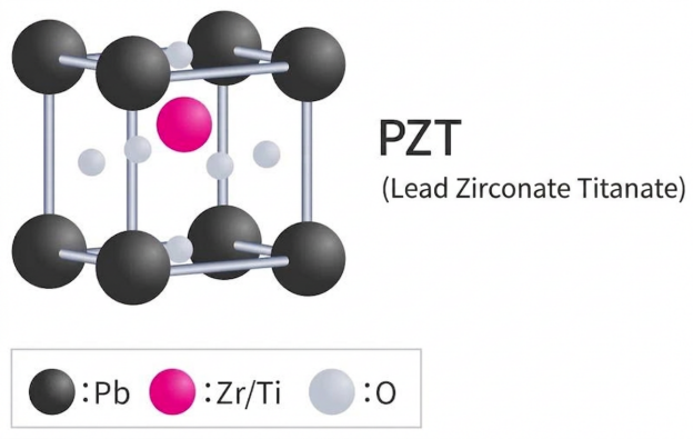
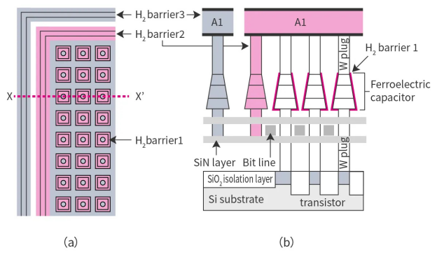
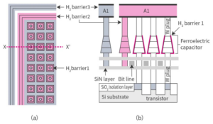
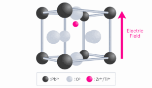
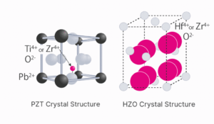
FeRAM(1) has a capacitor structure in which a PZT(2) ferroelectric layer is sandwiched between upper and lower electrodes. This configuration provides reliable data retention as well as fast read and write operation, owing to the ferroelectric polarization characteristics of the PZT film.
(1) FeRAM: Ferroelectric Random Access Memory
(2) PZT: Lead zirconate titanate
Challenges in FeRAM Mass Production
As FeRAM technology advanced toward commercial mass production, the method for forming PZT ferroelectric films became a key focus. At that time, the sol-gel method—a chemical solution-based process—was widely used. However, its limitations in throughput and process stability became evident when scaling to production.
As an alternative, sputtering, a type of physical vapor deposition (PVD), was investigated for its superior scalability and compatibility with semiconductor manufacturing lines. In this method, plasma is generated in a vacuum to eject atoms from a target material, which are then deposited onto a substrate to form a thin film. Since PZT targets are insulating, radio-frequency (RF) plasma is employed instead of the direct-current (DC) plasma commonly used for conductive materials.
The sol-gel process involves film formation through a transition from a sol state—where fine particles are dispersed in a liquid—to a gel state, forming a solidified network structure. While suitable for laboratory-scale fabrication, it posed challenges for process uniformity and productivity in large-scale manufacturing.
Engineering Innovations for Sputtering-Based Mass Production
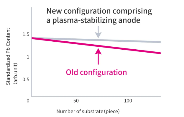
At the initial stage of adopting sputtering for PZT film formation, several technical challenges were identified. These included difficulties in controlling PZT film composition and maintaining stable plasma conditions during deposition.
To overcome these issues, dedicated mass-production equipment was co-developed with an equipment manufacturer (ULVAC). This effort enabled both stable plasma operation and precise control of film composition, paving the way for reliable high-volume manufacturing.
The key technological innovations can be summarized as follows(3)(4)(5):
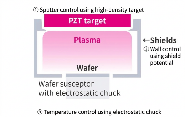
- Sputter rate stabilization using high-density ceramic targets
- Chamber wall conditioning via shield potential control
- Substrate temperature regulation using an electrostatic chuck
Through this development effort, engineers acquired in-depth knowledge of the internal configuration and behavior of the deposition equipment. This understanding proved instrumental in solving process-related challenges and advancing sputtering technology for ferroelectric applications.
(3) K.Suu, T.Masuda, Y.Nishioka and N.Tani, “Process Stability Control of Pb(Zr,Ti)03 Ferroelectric Thin Film Sputtering for FRAM Application”, Proceedings of the Eleventh IEEE International Symposium on Applications of Ferroelectrics, pp.19-22, 1998.
(4) Koukou Suu, Akira Osawa, Yutaka Nishioka and Noriaki Tani, “Stability Control of Composition of RF-Sputtered Pb(Zr, Ti)O3 Ferroelectric Thin Film”, Jpn.J.Appl.Phys. Vol.36, pp.5789-5792, 1997.
(5) K. Hidaka, S. Hashiguchi, S. Nagayama and P. Kim, “Properties of high-density (Pb, La) (Zr, Ti) O3 ceramics for sputtering target”, Vacuum Vol.59, pp.451-458, 2000.
Impact on FeRAM Manufacturing
The introduction of mass-production sputtering equipment enabled precise control of PZT film composition and significantly enhanced the reliability of FeRAM devices. This represented a major step forward in making FeRAM a practical and commercially viable memory technology.
The expertise accumulated during this development continues to play a vital role in current manufacturing processes. Importantly, the development philosophy—emphasizing a deep understanding of both process and equipment—has become deeply embedded within the organization.
Even today, engineers maintain a comprehensive perspective on the entire manufacturing process, including the equipment itself, and address technical challenges through a holistic, system-level approach. This mindset continues to drive innovation in FeRAM technology.
Summary
The evolution of FeRAM technology has been marked by continuous innovation in materials, processes, and manufacturing systems. The transition from sol-gel methods to sputtering-based deposition represents a key milestone in achieving scalable and reliable production of PZT ferroelectric films.
Building on these achievements, further advancements are anticipated in both device performance and manufacturing efficiency. By passing on accumulated technical knowledge to the next generation of engineers, continued progress in FeRAM technology is expected, supporting its expanding role in future memory applications.