SRAM Buffer Reduction Techniques: Optimizing Data Structures through Direct FRAM Writing
This guide explains the challenges and solutions for reducing SRAM buffers in embedded devices. It introduces a design method that utilizes direct writing to FRAM (FeRAM, ferroelectric memory) to optimize the data structure, thereby eliminating intermediate buffers and simultaneously reducing power consumption and memory usage.
Design Background for Reducing SRAM Buffers
In embedded devices, SRAM capacity is limited, and simultaneous operation of communication, control, and computation leads to contention of temporary buffers. Continuous logging and sensor recording increase copying, leading to stack exhaustion and fragmentation. Buffer reduction is crucial for both performance and reliability. Especially in low-power MCUs, external memory bandwidth is limited, and unnecessary buffering worsens latency and power consumption.
Constraints on SRAM Resources in Embedded Systems
SRAM is frequently used for interrupt handling and DMA work areas due to its low-latency random access. However, its capacity is small, and the stack and heap compete in the same space. Fixed allocation of temporary areas for communication stacks and encryption reduces available memory, and misestimating the maximum stack size can lead to corruption at boundary conditions. Furthermore, the indiscriminate use of C language automatic variables and temporary arrays causes peak usage to fluctuate depending on the execution path. The more safety margin is taken, the more strained SRAM becomes, forcing a decision between reducing functionality and adding external RAM.
Challenges Caused by SRAM Buffer Bloat
Increasing the buffer size reduces data loss, but each time data is copied from the receive buffer to the processing buffer and then to the storage buffer, it consumes memory bandwidth and CPU time. In MCUs with small caches, copying translates directly into latency, causing jitter in periodic tasks and deadline misses. In addition, power consumption increases, affecting heat and battery life. Furthermore, handling buffer boundaries becomes more complex, making it easier for off-by-one errors (incorrect boundary values) and insufficient mutual exclusion to creep in. During debugging, the content changes at each stage, making it difficult to track down the location of the problem.
Limitations of Traditional SRAM Reduction Approaches
Static optimizations such as reducing type width and placing constants in flash are effective, but temporary areas remain in streaming processing where input data fluctuates. Ring buffers also have difficulty reducing peak usage, and compression increases computational complexity and delay. Furthermore, dynamic allocation creates fragmentation, and the worst-case scenario becomes apparent during long-term operation. On the other hand, if the buffer size is made too small, retransmission control and other measures are required to prevent data loss, resulting in increased code size and verification effort.
FRAM Direct Writing Technology Fundamentals
FRAM is non-volatile yet boasts a write speed close to SRAM, allowing overwriting without prior erasure. This characteristic enables configurations that directly save data without temporary storage. By treating FRAM not merely as external storage but as a data space during execution, buffer reduction is achieved.
FRAM Writing Characteristics and Differences from SRAM
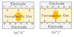
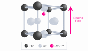
FRAM utilizes the polarization reversal of ferroelectric materials, eliminating the need for block erasure like flash memory and enabling byte-level random writing. It also has high rewrite endurance, making it suitable for frequent updates. On the other hand, SRAM is volatile and requires standby power, but has minimal latency. While FRAM involves a slight increase in write current and peripheral circuit constraints, it achieves both data retention and high speed. Particularly in logging applications, it can persist data immediately after reception, eliminating the need for dual buffers. The absence of erasure waiting results in less latency variation, making it suitable for real-time control.
Design Techniques for Treating FRAM as Memory Space
In MCUs equipped with built-in FRAM, data sections can be placed in FRAM using linker scripts and updated directly via pointers. Even external FRAM can be treated like an array if abstracted at the driver layer. The key is to establish a direct writing path from the application layer, bypassing caches and buffers. Clearly define the timing of write completion and incorporate fail-safe procedures to prepare for power loss. In memory-mapped systems, include access permissions and protection mechanisms in the design to prevent erroneous writes.
Reliability and Durability in Direct Writing
While FRAM has a high number of rewrite cycles, it is not unlimited, so a distributed update design is necessary. Avoid localized concentration through log structuring and a wear-leveling scheme. Furthermore, to prepare for mid-updates during power loss, introduce atomic updates using header and data commit flags and checksums. Using error detection codes in conjunction allows for detection of corruption due to bus noise or momentary power interruptions.
Data Structure Optimization for SRAM Buffer Reduction
To fundamentally reduce SRAM, redesign the data flow rather than simply compressing capacity, eliminating intermediate buffers and multi-stage copies based on the premise of direct storage to FRAM.
Transition from Copy-Based Design to Zero-Copy Design
Traditionally, a two-stage approach was common: data was received and stored in SRAM, then formatted before being written to persistent memory. Replacing this approach with a direct-to-FRAM data path allows incoming data to be stored immediately after reception and eliminates the need for intermediate buffers. Directing pointers to the persistent memory and performing processing in place reduces the number of copies. Furthermore, setting the DMA transfer destination to FRAM reduces CPU intervention. Defining the smallest unit to maintain consistency and designing an update sequence that leaves no intermediate states are crucial. Zero-copy operation not only improves speed but also directly reduces peak SRAM usage.
Design Points for Persistent Data Structures
When using FRAM as main memory, a structure that prevents data inconsistency after power loss is required. Adopting fixed-length records or log structures and using append-only updates localizes the impact of corruption. Using a generation number or valid flag in the header and switching atomically is an effective technique. Additionally, variable-length data is managed with an index table to suppress fragmentation. This enables direct updates without a temporary formatting area on SRAM.
Performance, Power Consumption, and Area Trade-off Evaluation
While SRAM reduction contributes to reducing area and standby power, increased FRAM access frequency presents challenges in terms of write current and bus occupancy. Latency and current waveforms are verified through actual measurements to quantify the impact on periodic tasks. The copy time reduced by eliminating buffers is compared with the waiting time increased by direct writing. The optimal point is determined based on the overall system energy and response time, including minimizing buffer usage at the cache line level as needed.
FRAM Design Approach for Successful SRAM Reduction
To safely reduce SRAM using FRAM, a systematic migration approach is necessary, from selecting target buffers to evaluation and verification.
Identifying and Prioritizing Buffers for Reduction
First, the size, maximum usage, and update frequency of all buffers are identified, and their contribution to peak SRAM consumption is quantified. They are classified by application, such as logs, communications, and caches, and migration is considered starting with areas well suited to persistent storage, such as data saved immediately after writing. Real-time constraints and the impact of failures are evaluated, and a phased reduction plan is developed. Prioritizing based on numerical values allows for a limited verification scope while reliably reducing SRAM usage.
Technical Criteria for FRAM Applicability
FRAM applicability is determined by access frequency, write size, and acceptable latency. While durability is sufficient even with high-frequency updates, distributed writing should be considered if bus bandwidth is congested. If consistency requirements during power loss are stringent, design should assume A/B (double) buffering, and SRAM retention is an option for read-centric data. Environmental conditions such as temperature range and retention period should also be considered to avoid the risks of a wholesale replacement.
Design Checkpoints During Implementation
During implementation, linker settings, driver delay, and mutual exclusion control with interrupts should be checked. If interrupts occur during writing, critical sections should be clearly defined to prevent data corruption. Furthermore, error detection codes and backup areas should be provided, and recovery procedures should be implemented for abnormal conditions. During evaluation, long-term continuous writing tests and momentary power interruption tests should be conducted to confirm behavior under worst-case conditions. During the design review, the focus is on verifying the memory map and update sequence to achieve both SRAM reduction and reliability maintenance.
RAMXEED FeRAM Product Lineup